


1. INTRODUCTION
Matter exists in three states – solids, liquids and gases. Based upon electrical properties solids are classified as conductors, insulators and semiconductors. Semiconductors are neither conductors nor insulators. Germanium and silicon are semiconductors. They play a dominant role in semiconductor physics and they have revolutionised the field of electronics. The transistor invented in 1948 has placed in our hands portable radio receivers, record players etc. and played an important role for the development of computer industry. Micro electronic circuits or integrated circuits use a very thin slice of silicon crystal about 0.05 cm in thickness. It is called a silicon wafer. It is also known as chip. The various components such as resistors, capacitors, diodes, transistors, logic gates etc., can be grown over one such silicon chip.
2. CRYSTALLINE AND AMORPHOUS SOLIDS :
Solids are classified into two types.
(i) Crystalline solids : The crystalline solids are those in which atoms or molecules are arranged in a definite and regular way through out the body of the crystal and possess a definite external geometrical shape.
Ex :Sugar, wood, quartz etc.,
Properties of crystalline solids : By virtue of their structure, crystalline materials exhibit the following properties:
a) Atoms are arranged in a regular pattern. This pattern repeats itself at regular intervals in space. They have long – range order.
b) Crystalline solids are anisotropic, i.e. physical properties like conductivity, refractive index, velocity of sound, depend on the direction. They have different values in different directions.
c) Crystalline solids posses uniform chemical composition i.e., bonds between all the atoms or molecules are of equal strength.
d) Crystalline solids have sharp melting points. i.e., on heating, all the bonds get ruptured suddenly at a fixed temperature. Due to this, change of state from solid to liquid occurs suddenly.
(ii) Amorphous solids :
The amorphous solids are those in which atoms or molecules are arranged in an irregular manner and do not have definite external geometrical shape.
Ex : Glass, rubber, sulphur etc.,
Properties of Amorphous solids: a) The amorphous solids are isotropic i.e., they have same physical properties in all directions.
b) Amorphous solids do not possess uniform chemical composition. i.e., bonds between all atoms and molecules are not of equal strength.
c) Amorphous solids do not have sharp melting points. i.e., on heating, the weaker bonds get ruptured first and the stronger ones later on. Due to this, change of state does not occur at a fixed temperature.
3. CLASSIFICATION OF SOLIDS
On the basis of electrical properties, solids are classified into three types.
(i) Conductors : The substances which easily allow the electric current through them are called conductors
Ex : Gold, silver, copper, aluminium, all metals.
Properties of conductors :
1. Conductors have high electrical conductivity and thermal conductivity.
2. Conductors have positive temperature coefficient of resistance. i.e. with the increase in temperature, the resistance of the conductor increases.
(ii) Insulators : The substances which do not allow the electric current through them are called insulators.
They have negative temparature coefficient of resistance. i.e., with the increase in temperature resistance decreases.
Ex : Glass, wood, mica etc.,
Insulators have high resistivity and low electrical conductivity.
(iii) Semiconductors : The substances whose electrical properties lie in between conductors and insulators are called semiconductors.
Ex : Germanium (Ge) and silicon (Si)
Properties of semiconductors:
a) The resistivity of semiconductors is higher than that of conductors but lower than that of insulators.
b) They have negative temperature coefficient of resistance i.e. the electrical resistance of a semiconductor decreases with increase in temperature.
c) The electrical conductivity of a semiconductor can be increased by adding a small amount of suitable impurity. This is called doping
4. BAND THEORY OF SOLIDS
In case of a single isolated atom, there are discrete energy levels, 1s, 2s, 2p, 3s,…, that can be occupied by the electrons of atom, as shown in figure Fig (a).
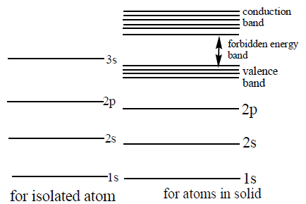
As isolated atoms are brought together to form a solid, various interactions occur between neighbouring atoms. As a result of this interaction, the higher energy levels are considerably affected i.e., the energy levels of the outer shell are slightly altered without violating Pauli’s exclusion principle. There will be splitting of a single energy level of an isolated atom into a large number of energy levels as shown in figure (b).
Since in a solid, many atoms (N =1023atoms/cm3) are brought together, the separation between N sub-levels (into which each discrete energy level splits due to interaction) is very small. For example, if there are 50 atoms in a piece of solid material, then there will be 50 levels of slightly different energies i.e., 50 energy
level diagrams would be superimposed on each other. Consequently, the split energy levels are almost continuous and are said to form an energy band.
Now, the energy bands in a solid correspond to the energy levels in an atom. An electron in a solid can have only those discrete energies that lie within these energy bands. These bands are, therefore, called allowed energy bands. These (allowed) energy bands are in general separated by some gaps which have no allowed energy levels. Energy bands occupied by the valence electrons is called valence band and is obviously the highest occupied band. Energy bands occupied by the conduction electrons is called conduction band. It is highest unfilled energy band. Electrons in conduction band are weakly bound to the nucleus.
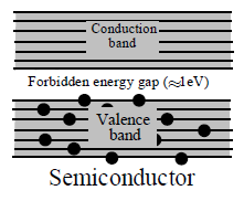
The energy gap between the valence band and conduction band is called the forbidden energy band.
5. INSULATORS, SEMICONDUCTORS AND CONDUCTORS
On the basis of band theory, the insulators, semiconductors and conductors are described as follows :
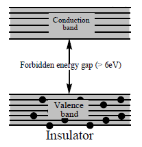
Insulators : In case of insulators, the forbidden energy gap between valence band and conduction band is large. The width of the forbidden energy gap in insulators is of order of 6 eV as shown in fig. In insulators, valence band is filled with electrons and they are bound very tightly to their parent atoms so the conduction band is empty. Due to large forbidden energy gap electrons cannot jump from valence band to conduction band.
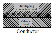
Conductors : In conductors, the valence band and conduction band overlap each other as shown in fig. In conductors the forbidden energy gap is 0 eV. The electrons in valence band can easily enter into the conduction band. A slight potential difference across the conductor cause the electrons to constitute electric current.
Semiconductors : In semiconductors, the forbidden energy gap between valence band and conduction band is very small as shown in fig. In germanium, the forbidden energy gap is 0.7 eV and in silicon, the forbidden energy gap is 1.1 eV. In semiconductors at 0K, there are no electrons in conduction band and the valence
band is completely filled with electrons so they behave as insulators at 0K. When a small amount of energy is supplied, the electrons can easily jump from valence band to conduction band.
|
S.No |
Conductors |
Semi Conductors |
Insulators |
|
1. |
In this, valence band and conduction band overlap each other |
In this, valence band and conduction band are separated by small forbidden gap. |
In this, valence band and conduction band are largely separated. |
|
2. |
Forbidden Energy gap = 0 eV |
Forbidden energy gap is in the order of 1 eV. |
Forbidden energy gap is in the order of 6 eV |
|
3. |
At room temperature conductivity is high |
At room temperature conductivity is intermediate. |
At room temperature conductivity is nil. |
|
4. |
Ex :- All metals |
Ex :- Ge, Si |
Ex :- Rubber, Glass, Mica. |
|
5. |
V.B & C.B over lap |
V.B is almost full C.B. is almost empty |
V.B. is completely filled C.B. is completely empty |
6. TYPES OF SEMICONDUCTORS
1) Intrinsic semiconductors.
2) Extrinsic semiconductors.
7. INTRINSIC SEMICONDUCTOR :
A semiconductor in an extremely pure form is known as intrinsic semiconductor.
Ex : Silicon (Si), Germanium (Ge)
The atoms of pure semiconductors are tetra valent.
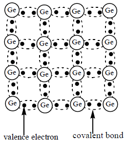
In their crystal lattice each atom forms four covalent bonds with its neighbouring atoms as shown in the figure. Due to this valence electrons are tightly bound. So crystal has low conductivity.
i.e., At 0K temperature, valence band is filled with electrons and conduction band is empty. Hence intrinsic semiconductor acts as an insulator at 0K.
As temperature increases covalent bonds between the atoms start breaking, hence electrons in the valence band get energy and jump into the conduction band. At that place in the valence band, a vacancy is created.
This vacancy of electron in the valence band is called a hole. ‘ Hole’ behaves like a positive charge and moves only in the valence band giving ‘ hole current ‘ [Ih]. The excited electrons in the conduction band move in the conduction band giving ‘ electron current [Ie].
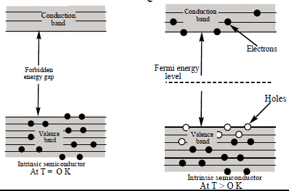
Under applied electric field the holes drift in the direction of electric field and electrons drift opposite to the direction of electric field with greater speed. Hence the current in semi conductor is due to both electrons as well as holes. In intrinsic semi conductors the number of electrons in the conduction band is equal to number of holes in the valance band i.e., ne = nh.
In this semiconductor, the average energy of electrons in conduction band is equal to the average energy of holes in valency band.
Fermi energy: The highest energy that an electron can have at 0K is called fermi energy. The level corresponding to fermienergy is called fermienergy level (or)
The average of energies of holes in the valance band and electrons in the conduction band is called fermi energy.
∴ Fermi energy level in intrinsic semiconductor is at the middle of the forbidden band.
The conductivity of intrinsic semiconductors is very less and their conductivity can be increased by adding impurity.
DOPING:- The process of adding impurity to a pure semiconductor crystal so as to increase its conductivity is called doping.
8. EXTRINSIC SEMICONDUCTORS
The semiconductors with impurities are called extrinsic semiconductors. Extrinsic semiconductors are of two types. They are p – type and n – type semiconductors.
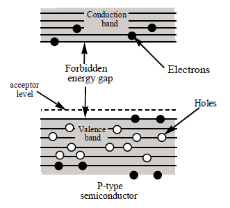
9. P – TYPE SEMICONDUCTOR
When a few atoms of the trivalent elements (boron, aluminium, gallium or indium) are added to the pure germanium or silicon crystal, the resulting crystal is called p – type semiconductors. This impurity atom is called acceptor impurity
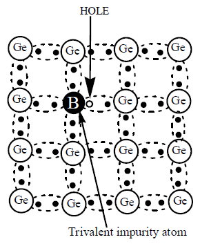
When trivalent boron is added to pure germanium crystal each atom of boron form three covalent bonds with the surrounding germanium atoms. In the fourth covalent bond, only germanium atom contributes one valence electron and there is deficiency of one electron which is called a hole. Therefore, for each boron atom added, one hole is created.
Acceptor level: The energy level occupied by the hole due to trivalent doping which lies very close to valance band is called acceptor level
Doping of small amount of boron provides millions of holes. The energy band description of P-type semiconductor is shown in fig. The addition of trivalent impurity, produces a large number of holes in the valence band. However, there are few electrons in the conduction band due to thermal energy associated with room temperature. In the incomplete covalent bond, the remaining fourth electron of germanium atom also tries to form a covalent bond. Actually it does by taking the advantages of the thermal motion. It steals an electron from the neighboring germanium atom. Due to this stealing action, a hole is created in the adjacent atom. This process continues and the hole moves about in a random way due to thermal effects.
(i) In p-type semiconductors the number of electrons in conduction band are less than the number of holes in the valence band so holes are called majority charge carriers and electrons are called minority charge carriers
(ii) The p-type semiconductor is electrically neutral because the creation of extra hole does not result in removal of any charge
(iii) In p-type semiconductors the average energy of holes in valence band is more than that of average energy of electrons in conduction band.
(iv) The fermi energy level in p-type semiconductors is just above the valence band.
(v) In p – type semiconductors, the ratio of number of electrons in conduction band to the number of holes in valence band increases with increase of temperature, but this ratio is always less than one.
(vi) The relation between the electron density ne, hole density nh and the density of intrinsic charge carriers ni is
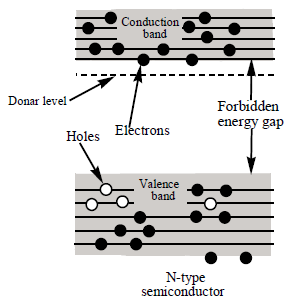
10. N – TYPE SEMICONDUCTOR :
When a few atoms of the pentavalent elements (nitrogen, phosphorus, arsenic, antimony and bismuth) are added to the pure germinium or silicon crystal, the resulting crystal is called N-type semiconductor .
This impurity is called donar impurity

When pentavalent arsenic atom is added to pure germanium crystal as shown in fig. The arsenic atom fits in the germanium crystal and it forms four covalent bonds with the surrounding four germinium atoms. The fifth electron of arsenic atom is not covalently bonded but it is loosely bound to the parent arsenic atom.
Donor level : The energy level occupied by an electron donated by pentavalent impurity which lies very close to conduction band is called donar level. This electron is available as a carrier of current. The amount of energy needed to detach this fifth valence electron from impurity atom is very small. This energy is provided with thermal agitation at room temperature. Such a liberated valence electron is then free to move in the crystal lattice. Although each arsenic atom provides only one free electron yet an extremely small amount of doping of arsenic impurity provides millions of free electrons.
(i) In N-type semiconductor the number of electrons in the conduction band is more than the number of holes in valence band, so electrons are called majority carriers and holes are called minority carriers.
(ii) In N-type semiconductor the average energy of electrons in conduction band is more than the average energy of holes in valance band.
(iii) In N-type semiconductor the fermi energy level is just below the conduction band.
(iv) N-type semiconductor is electrically neutral. Because the creation of extra electron does not result in additional charge of the atom
(v) The relation between the electron density ne, hole density nh and the density of intrinsic charge carriers
Note : If the forbidden energy gap is ‘x’ eV, the wave length of the photon required to excite an electron from valence band to conduction band is given by
Whenever a covalent bond breaks an electron hole pair is formed.
When a valence electron combines with a hole a covalent bond is formed and at the starting point of the electron a hole is formed.
If a conduction electron combines with a hole a covalent bond is formed without the formation of hole anywhere else.
11. MOBILITY OF CHARGE CARRIERS
Electric current is due to the movement of charge carriers. In a semiconductor, charge carriers are electrons in the conduction band and holes in the valence band. Due to thermal agitation, they move randomly in all directions and hence the net current in any direction is zero.
When an electric field E is applied across a semiconductor, every charge carrier experiences a force due to electric field and drifts in the direction of the force. Thus, a charge carrier acquires an average velocity which is called the drift velocity. It gives rise to the drift current.
The average drift velocity per unit electric field is called the mobility of a charge carrier.
∴ mobility μ =
Where vd is the drift velocity and E is the applied electric field.
Note: Mobility of electrons is more than that of holes because mobile electrons are in conduction band and holes are in valence band.
Mobility is a property of the semiconductor itself. It does not depend upon the doping concentration. The mobility of an electron or hole generally decreases with increasing temperature.
12. THE P-N JUNCTION DIODE :
i) When a semiconducting material such as silicon or germanium is doped with trivalent impurity on one side and pentavalent impurity on the other side we obtain a p-n junction. The plane separating the two regions is called a junction.
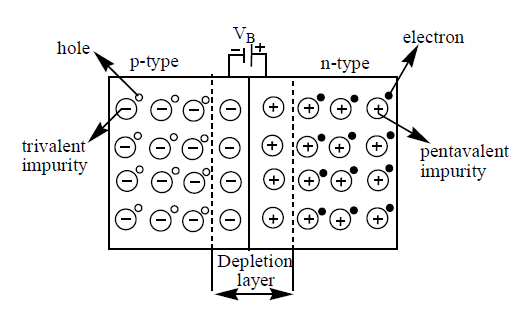
ii) Near the junction, the free electrons from n-region migrate towards p-region and the holes in p-region migrate towards n-region. This process is known as diffusion. This diffusion is due to concentration gradient.
iii) Due to diffusion, positive ions are left over in n-region and negative ions are left over in p-region, near the junction. These ions are immobile.
iv) Due to the immobile ions on either side of the junction an internal electric field is formed at the junction which is directed from n- region to p – region.
v) A region of no charge carriers that is formed at p-n junction due to the combination of electrons and holes is called depletion layer.
vi) The thickness of the depletion layer is of the order of m.
vii) When the depletion layer is sufficiently built up, it prevents the further diffusion of electrons from n side to p side and holes from p to n side i.e. it acts as a barrier.
viii) The potential difference across the barrier is called potential barrier or contact potential It behaves as a pseudo battery.
ix) The potential barrier for silicon is around 0.7 volts and for Germanium it is around 0.3 volts.
x) The potential barrier value lies in between 0.1 to 0.7 volts, which depends on
(a) the nature of semiconductor,
(b) doping concentration
(c) temperature of the junction.
xi) If V is the barrier potential and d is the thickness of the depletion layer, then the electric field intensity across the junction is
from n side to p side.
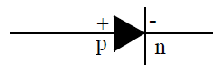
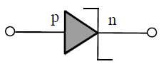
The below figure represents the circuit symbol of p-n junction diode. The arrow head shows the direction of the conventional electric current
Diffusion current: Due to the difference in concentration of charge carriers, holes from p-side diffuse towards n-side and electrons from n-side diffuse towards p-side. The movement of these charge carriers across the junction causes a current. This current is called diffusion current. Diffusion current is from p-side to n-side
Drift current: If an electron – hole pair is created in the depletion region, the electron is quickly pushed by the electric field towards the n-side and the hole towards the p-side. There is almost no chance of recombination of a hole with an electron in the depletion region. As electron-hole pairs are continuously created in the depletion region, there is a regular flow of electrons towards the n-side and of holes towards the p-side. This makes a current from the n-side to the p-side. This current is called drift current.
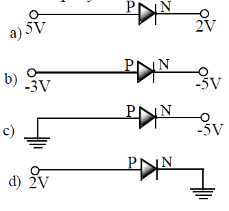
13. FORWARD BIAS
When the positive terminal (high potential) of a battery is connected to P – type semiconductor and the negative terminal (low potential) of the battery is connected to N- type semiconductor. Then the junction diode is said to be in forward bias as shown in fig. In forward bias the applied potential establishes an electric field opposite to the potential barrier.
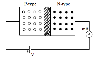
In case of forward bias, the holes from P – type semiconductor are repelled by the positive terminal of battery towards the junction and simultaneously, the electrons in N – type semiconductor are repelled by negative terminal of battery towards junction. In forward bias the width of the depletion layer decreases. If V is the external applied voltage and VB is the barrier potential then the net potential in forward bias is (VB V). When the battery voltage is high it gives sufficient energy to these carriers to overcome the potential barrier at the junction. Then the current in diode sharply rises.
1) In forward bias current is mainly due to flow of majority charge carriers and it is of order of milli amperes.
2) In forward bias the resistance offered by the diode is less.
3) In forward bias the current flow through the diode is mainly due to diffusion of charge carriers.
The below diagrams show forward bias of p-n junction diode.
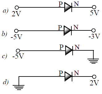
14. REVERSE BIAS
When the positive terminal (high potential) of a battery is connected to N-type semiconductor and the negative terminal (low potential) of the battery is connected to P-type semiconductor, then the junction diode is in reverse bias.
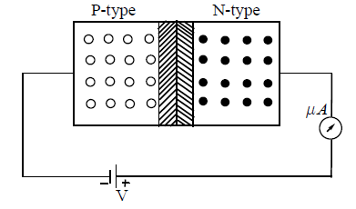
In reverse bias, the holes in P-type semiconductor are attracted by the negative terminal of the battery and they move away from the junction, simultaneously electrons in N-type semiconductor are attracted by the positive terminal of the battery and they move away from the junction. The width of the depletion layer increases in reverse bias. If V is the applied voltage and VB is the barrier potential, then the effective barrier potential in reverse bias is (VB + V). In reverse bias diffusion of electrons from N-side to P-side and holes from P-side to N-side is more difficult and diode will not allow electric current through it. Due to minority carriers ( electrons in P-type semiconductor and holes in N-type semiconductor) a small current flows. The
current in germanium diode is of order of μA and in silicon diode it is in the order of nA. The resistance offered by the diode in reverse bias is high.
In reverse bias the flow of current through diode is mainly drift current.
The below diagrams show reverse bias of p-n junction diode.
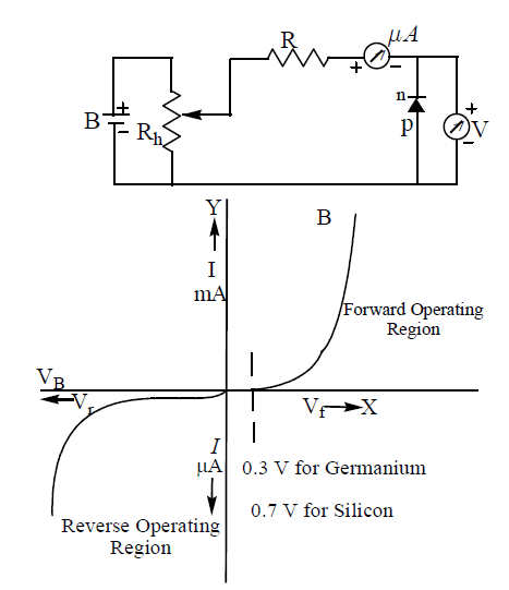
15. VOLTAGE-CURRENT (V-I) CHARACTERISTICS OF A P-N JUNCTION DIODE :
The V-I characteristics of a P-N-junction diode is the curve drawn between voltage across the diode on X-axis and current passing through the diode on Y-axis.
(i) Forward Bias : In forward bias of a P-N junction, P -side is connected to the positive terminal while the N – side is connected to the negative terminal of a battery. The potential at P-N junction can be varied with the help of potential divider. At some forward voltage (0.3V for Ge and 0.7 V for Si) the potential barrier is almost eliminated and current starts flowing. This voltage is known as threshold voltage (Vth) or cut – in voltage or knee voltage. It is practically same as barrier voltage VB . As the forward applied voltage increases beyond threshold voltage, the forward current rises exponentially. This forward current is due to majority charge carriers in p-n junction diode.
(ii) Reverse Bias : For the reverse bias of P-N junction P-side is connected to the negative terminal and Nside is connected to the positive terminal of a battery. The reverse potential at P-N junction can be varied with the help of potential divider. In this case the junction resistance becomes very high and no current should flow through the circuit. However, in practice, a small current of the order of μA flows in the circuit due to minority charge carriers as applied voltage is forward bias for minority charge carriers. This is known as reverse current. As the reverse voltage is increased from zero, the reverse current quickly rises to its maximum or saturation value. If the reverse voltage is further increased, the kinetic energy of electrons
(minority carriers) become so high that they knock out electrons from the semiconductor atoms. At this stage breakdown of diode occurs and there is a sudden rise of reverse current. Now the diode is destroyed permanently.
The sharp increase in current under breakdown conditions are due to following two mechanisms.
(i) Avalanche breakdown : This type of breakdown takes place when both sides of junction are lightly doped and consequently the depletion layer is large. In this case, the electric field across the depletion layer is not so strong. Here, the minority carriers are accelerated by the applied voltage and collide with the semiconductor atoms in the depletion region. Due to the collision with valence electrons covalent bonds are
broken and electron hole pairs are generated. These new carriers so produced acquire energy from applied potential and in turn produce additional carriers. This forms a cumulative process called avalanche (or flood) multiplication. The breakdown is called avalanche breakdown.
(ii) Zener breakdown : Zener breakdown takes place in very thin junction, i.e., when both sides of junction are heavily doped and consequently the depletion layer is narrow. When a small reverse bias voltage is applied, a very strong electric field (above 107 V/m) is set up across the thin depletion layer. This field is strong enough to break or rupture the covalent bonds. Now extremely large number of electrons and holes
are produced which constitute the reverse saturation current (zener current). Zener current is independent of the applied voltage. This occurs in heavily doped diodes at low reverse bias voltages.
Application : The current flows through the diode in the below circuit is
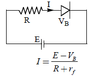
Where R = external resistance, rf = resistance of diode in forward biase, VB = barrier potential.
Application :
i) Power developed across the diode =
ii) Power developed across the resistor =
Application:
The potential barrier existing across an unbiased p-n junction is VB volt.
i) The minimum kinetic energy required by a hole to diffuse from the p-side to the n-side is ‘eVB‘
ii) If the junction is forward biased at V volt. Then the minimum kinetic energy required by a hole to diffuse from the p-side to the n-side is e(VB V )
iii) If the junction is riverse biased at V volt. Then the minimum kinetic energy required by a hole to diffuse from the p-side to the n-side is e(VB + V).
Note5.8: The above formulae are true even for an electron diffusing from n–side to p–side.
16. JUNCTION DIODE AS RECTIFIER :
Rectification: The process of converting an alternating current into a direct current is called rectification.
Rectifier: The device used to convert an alternating current into a direct current is called rectifier. A p-n junction diode can be used as a rectifier because it permits current in one direction only.
17. HALF WAVE RECTIFIER :
A half wave rectifier can be constructed with a single diode ‘D’ as shown in figure.
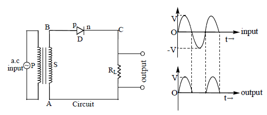
A half wave rectifier rectifies only one half cycle of the ac input. An ac source along with a step down transformer is connected to a load resistance through a p-n junction. The potential at the point A is taken to be zero. The potential at B varies with time as V = V0 sin (ωt+). During the positive half-cycle, V > 0 and B is at a higher potential than A. In this case, the junction is forward-biased and current passes through the
load resistance in the direction C to A.
During the negative half-cycle. V< 0 and the potential at the point B becomes smaller than that at A. The junction is thus reverse-biased and offers a large resistance during this half-cycle and there is only a negligible current in the circuit.
Thus current flows through the diode during positive half cycles only. Current flows in RL only in one direction. So a half wave rectifier gives discontinues and pulsative DC output as shown in figure.
The number of DC pulses per second is equal to the frequency of the applied AC.
Efficiency of half wave Rectifier : Efficiency of a rectifier is the ratio of dc power output to the ac power input.
Efficiency of rectifier =
For half wave rectifier =
Here rf is diode forward resistance and RL is load resistance
In a half wave rectifier, a maximum of 40.6% of ac power is converted to dc power.
18. FULL WAVE RECTIFIER :
A rectifier which rectifies both halves of the ac input is called full wave rectifier. A full-wave rectification can be achieved by using two diodes as shown figure. This circuit has two diodes and and a transformer known as centre tap transformer.
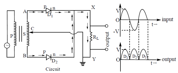
In centre tap transformer, the secondary is wound into two equal parts. Voltage at A (input of diode D1) and B (input of diode D2) with respect to centre tap C are out of phase with each other. Suppose the input voltage to A at any instant is positive, it is clear that, at that instant, voltage at B being out of phase will be negative and vice versa. During the positive half cycles of ac input, diode D1 is forward biased and diode D2 is reverse biased and D2 will not conduct and the current flows through the load resistance RL due to D1 . Similarly during negative half cycles of ac input, diode D2 is forward biased and D1 is reverse biased and will not conduct and the current flows through the load resistance RL due to D2. Hence, current flows through the load resistance during both the half cycles and in the same direction. Thus, using full wave rectifier, the output is continous but pulsating as shown in Figure. The pulsating current can be made smooth using filter circuits.
The number of dc pulses per second of the output is equal to twice the frequency of the ac input.
Efficiency of full wave Rectifier:
Efficiency of a rectifier is the ratio of dc power output to the ac power input.
Efficiency of the rectifier
For full wave rectifier =
Here rf is diode forward resistance and RL is load resistance
In a full wave rectifier, a maximum of 81.2% of ac power is converted to dc power.
Note: It is clear from the figure that current always flows from X to Y in load resistor RL either when D1 conducts or when D2 conducts (along the direction of arrows as shown in figure)
19. THE ZENER DIODE
The properly doped P-N junction diode which has sharp breakdown voltage when operated in the reverse bias condition is called Zener diode.
For a heavily doped diode, the depletion layer is very narrow. When the reverse bias voltage across the diode is increased, intense electric field ( 3 ⨯ 107 V /m) setup across the depletion layer breaks the covalent bonds in it. It produces a large number of electron-hole pairs resulting in a sharp increase in reverse current.
(a) Voltage – Current Characteristics of a Zener diode :
The voltage -current characteristics for a Zener diode are shown in figure. In forward bias, its characteristics are similar to that of an ordinary p-n junction diode. When reverse biased, a small reverse saturation current flows through it which remains approximately constant until a certain critical voltage, called breakdown voltage, is reached. At this voltage, the reverse current IR increases sharply to a high value. This break down voltage VZ is called the Zener voltage and the reverse current is called Zener current. The Zener voltage depends on the amount of doping. A heavily doped diode has a narrow depletion layer and consequently a lower breakdown or Zener voltage.
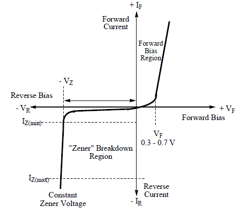
On the other hand, if the diode is lightly doped, the breakdown of the junction will occur at higher voltage. For breakdown voltages below 6 volt, the Zener effect is predominant. For higher voltages, the avalanche multiplication is effective. Between 5 and 8 volts both effects are present.
When a Zener diode is operated in the breakdown region, the voltage across the diode remains constant (equal to VZ) for the large change of the reverse current. The voltage across a Zener diode thus serves as a reference and the diode is used as a voltage reference device for stabilizing a voltage at a predetermined value.
The circuit symbol for a Zener diode is shown in figure. It is similar to that of an ordinary diode except that the bar is turned into Z-shape.
20. ZENER DIODE AS A VOLTAGE REGULATOR
A device used to give constant output voltage even when the input voltage to it varies or load resistance to it change is called voltage regulator or voltage stabilizer.
A simple Zener diode voltage stabilizer circuit is shown in figure. This circuit is used to maintain a constant voltage across a load resistor RL inspite of variations in either the supply voltage or the load current (due to a change in the load resistance) or both. In the circuit, the input is a d.c. voltage whose voltage variations has to be regulated. The P-side of zener diode is connected to the negative terminal of the input voltage and N-side is connected to the terminal to the positive.
The value of ‘RS‘ is selected in such a way that in the absence of load ‘RL‘ maximum safe current flows through the diode. Now consider that the load is connected across the diode. The load draws a current IL. The current thought the diode falls by the same amount but the voltage drop across the resistance ‘RL‘ almost remains constant.
If input voltage increases with load resistance fixed, then input current I increases. This results in equal increase of zener current (IZ) without change in load current. With increase of zener current, voltage (VZ) across zener diode does not change. Thus voltage across the Zener diode remains constant even if input voltage is increased.
If input voltage fluctuations occur, the series resistance ‘RS‘ controls the output voltage fluctuations so as to maintain constant voltage across the load.
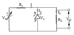
If the load resistance increases, with the supply voltage fixed, then load current IL decreases and the Zener current IZ increases by an equal amount. Thus the Voltage V0 = VZ across the load will remain constant.
Let I be the current drawn from the source, IZ is the current passing through the Zener diode and IL is the current passing through the load resistance
If VS is the voltage across the series resistance and VZ is the zener voltage then
But
The current passing through the zener diode is
21. USES OF SEMICONDUCTOR DIODES:
1 p-n junction diodes are minute (very small in size). Therefore, they are used in micro circuits.
2 As they are solid state devices, no evacuation is needed like vacuum tubes.
3 Their efficiency is more than that of vacuum tubes.
4 They are also quite strong and sturdy.
5 Usually , they have long life
6 There is no filament heating and consequent power loss.
7 These can be prepared to function over wide voltage ranges and to give very large rectified currents.
22. TRANSISTORS
The transistor was invented in 1948 by J. Bardeen, W.H. Brattain and W. Shockley.
A junction transistor is simply a sandwich of one type of semiconductor material between two layers of the other type. Accordingly, there are two type of transistors:
1. n–p–n transistor
2. p–n–p transistor
When a layer of p–type material is sandwiched between two layers of n–type material, the transistor is known as n–p–n transistor. Similarly, when a layer of n–type material is sandwiched between two layers of p–type material, the transistor is known as p–n–p transistor. Transistors are made either from silicon or germanium crystal. The symbols employed for n–p–n and p–n–p transistors are also shown in fig.
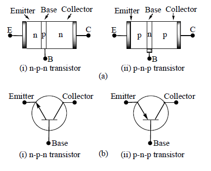
In symbols of transistors arrowhead is always at the emitter. The direction indicates the conventional direction of current flow, i.e. in case of n–p–n transistor it is from base to emitter (base is positive with respect to emitter) while in case of p–n–p transistor it is from emitter to base (emitter is positive with respect to base).
Although the two outer regions are of the same type but they cannot be interchanged. The reason is that the two regions have different physical and electrical properties.
The three sections of the transistor are emitter (E), base (B) and collector (C).
(i) Emitter: The main function of this region is to supply majority charge carriers (either electrons or holes) to the base and hence it is heavily doped in comparison to other regions.
(ii) Base: The middle section of the transistor is known as base. This is very lightly doped and is very thin (10–6m) as compared to either emitter or collector so that it may pass most of the injected charge carriers to the collector.
(iii) Collector: The main function of the collector is to collect majority charge carriers through the base.
This is moderately doped.
23. BASIC TRANSISTOR CIRCUIT CONFIGURATIONS :
In any electronic circuit or device, there has to be two terminals for input and two terminals for output. In a transistor, only three terminals are available, viz., Emitter (E), Base (B) and Collector (C). Therefore, in a circuit the input / output connections have to be such that one of these (E, B or C) is common to both the input and the output. Therefore, the transistor can be connected in anyone of the three following
configurations.
1) Common base (CB) configuration ,
2) Common emitter (CE) configuration.
3) Common collector (CC) configuration.
24. COMMON BASE CONFIGURATION :
In this configuration base is common to both input and output. Base terminal is earthed and input is given across emitter–base and output is taken across collector–base as shown in figure.

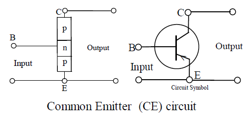
25. COMMON EMITTER CONFIGURATION:
In this configuration emitter is common to both input and output. The emitter is earthed and input is given across base – emitter and output is taken across collector–emitter as shown in figure.

26. COMMON COLLECTOR CONFIGURATION:
In this configuration collector is common to both input and output. The collector is earthed and input is given across base – collector and output is taken across emitter -collector as shown in figure.
5.27 WORKING OF p-n-p TRANSISTOR:-
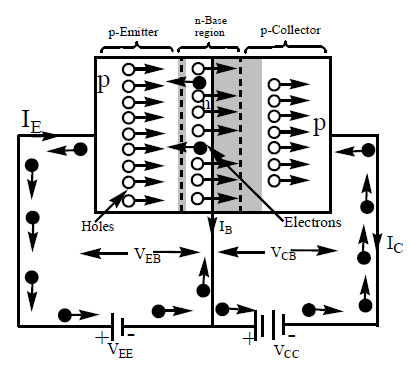
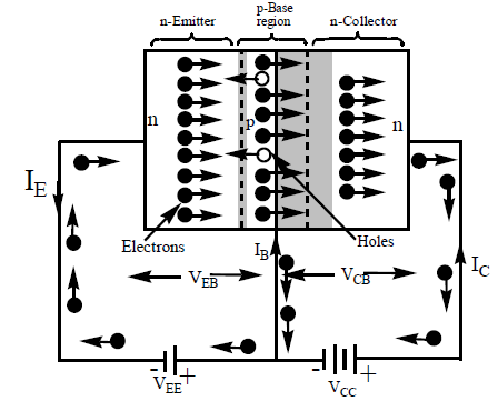
The given circuit shows the p-n-p transistor with batteries connected in proper way for common base configuration. The emitter–base junction is forward biased with positive end of the battery to the emitter and negative to the base. The collector–base junction is reverse biased with collector negative with reference to the base.
The holes in the emitter p – region are repelled by the positive polarity and after crossing the emitter – base junction enter the base region. Flow of holes in emitter region constitute the emitter current (IE). As base is lightly doped, majority of the holes drift across the base without combining with electrons.
Except few that are lost by recombination constituting base current (IB), majority of the holes penetrate through the collector junction and enter the collector region.
The collector terminal at the right end rapidly sweeps the holes that enter the collector region causing a large current.
In emitter covalent bond breaks down, liberating electron that enters the positive terminal of the emitter battery and the new hole created then moves towards the collector. As each hole reaches the collector electrode, an electron is emitted from a negative battery terminal of collector and neutralizes the hole. This constitute collector
current (IC).
A continuous supply of holes injected into the emitter junction flows across the base region to the collector junction where they are collected by the negative collector electrode. Thus current conduction within the pn – p transistor takes place by hole conduction. In the external circuit only electrons carry out the conduction.
The relation between the emitter current (IE), base current (IB) and collector current (IC) is given by.
IE = IB + IC.
The practical value of current that reaches the collector ranges from 95 to 99 percent of current leaving the emitter. The current gain (α) is defined as the ratio of small change in collector current to small change in emitter current. i.e., , α is less than unity.
28. WORKING OF n-p-n TRANSISTOR:
The above diagram shows the n p n transistor with batteries connected in proper way for common base configuration. The emitter–base junction is forward biased with negative end of the battery connected to the emitter and positive to the base. The collector–base junction is reverse biased with collector positive with reference to the base.
a) The electrons in the left n – region (emitter) are repelled by the negative polarity and after crossing the emitter – base junction (called emitter junction) enter the base region. Flow of electrons in emitter region constitute the emitter current (IE). As base is lightly doped, majority of the electrons drift across the base with out combining with holes there.
b) Except few that are lost by recombination constituting base current (IB), majority of the electrons penetrate through the collector junction and enter the collector region.
c) The collector terminal at the right end rapidly sweeps the electrons that enter the collector region causing a large current.
These electrons liberated in emitter are moved towards the collector and are drawn by the positive electrode of the battery at collector and finally reach the emitter terminal. Thus the current flows in the circuit continuously. In the external circuit also electrons carry out conduction.
The relation between emitter, base and collector currents is
Current gain
In comparison between n p n and p n p transistors, n p n transistors are faster in action than p n p transistors because mobility of electrons is more than that of holes.
29. CHARACTERISTICS OF A TRANSISTOR IN CE – CONFIGURATION:
Any variation in the voltage on the input and output sides results in a change in the input and output currents respectively.
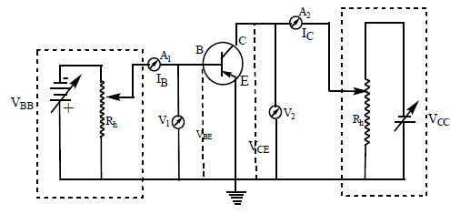
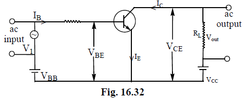
A p-n-p transistor is connected in the common emitter configuration as shown in the circuit figure.
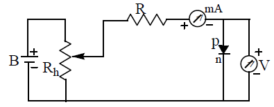
To activate the transistor, the emitter junction is forward biased and collector junction is reverse biased. This is achieved by giving positive polarity to the emitter (p – type) and negative polarity to the base (n – type) through a variable source VBB. This is called the input circuit. It is forward biased. To measure base current (IB) a micro ammeter A1 and to measure the potential difference VBE, between base and emitter a voltmeter V1 are connected.
The collector – base junction is reverse biased by giving negative polarity to collector (p – type) and positive to emitter through a variable source ‘VCC’ . This is called output circuit, and is reverse biased. To measure collector current (IC) a milliammeter A2 and to measure potential difference VCE across collector and emitter , a voltmeter ‘V2’ are connected.
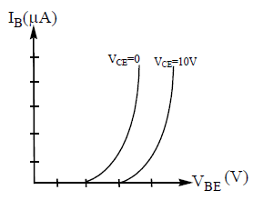
i) Input characteristics :- The graph drawn between base current [IB] on y – axis and base emitter voltage [VBE] on x – axis, keeping the collector voltage [VCE] constant, is called input characteristics.
The output voltage VCE is fixed (say at zero volt). The input voltage VBE is changed in steps (say 0.1 V) upto 1 volt and the corresponding base current IB is noted down. We observe that, with the collector shorted to the emitter and the emitter forward biased, the input characteristic is essentially that of a forward biased diode.
This process is repeated for different values (say 5V, 10V etc.) of VCE. Curves between VBE and IB drawn are shown in the Figure. These curves are called as input characteristic curves of transistor.
The characteristics are similar to that of a forward biased diode. The dynamic resistance, or input resistance,
ii) Output characteristic :
The graph drawn between output current [IC] on y -axis and output voltage [VCE] on X-axis, keeping the base current (IB) constant is called output characteristics.
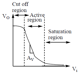
Base current (IB) is fixed at a small value (say 10 μA), the collector emitter voltage VCE is steadily increased from zero in regular steps (say 0.5V) upto 10V and the corresponding collector currents IC are noted. This process is repeated for different values of base current (say 20 μA, 30 μA etc). Curves between VCE and IC for different values of IB are drawn in the Figure. These curves are known as output characteristics. From these characteristic curves, it is evident that IC depends almost entirely on Ib and will not vary much with VCE except when VCE is very small. From the out put characteristics Figure, we define three different regions of operations of a transistor namely,
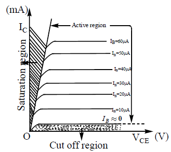
1) Saturation region: In this region the collector current becomes almost independent of the base current. This happens when both junctions are forward biased.
2) Cut off region: In this region the collector current is almost zero. This happens when both the junctions are reverse biased.
3) Active region: In this region collector current (IC) is many times greater than base current (IB).
A small change in input current (ΔIB) produces a large change in the output current (ΔIC). This happens when emitter junction is forward biased and collector junction is reverse biased.
The ratio of change in collector emitter voltage (ΔVCE) to the change in collector current (ΔIC) at constant base current (IB) is called output resistance.
Note: The transistor works as an amplifier when operated in the active region.
When the transistor is used in the cut off (or) saturation state, it acts as a switch.
30. CURRENT GAIN [β] IN CE MODE
Current gain in CE mode is defined as the ratio of small change in the collector current to a small change in the base current, keeping the collector–emitter voltage constant when the transistor is in active region
The value of β is about 20 to 200.
31. CURRENT GAIN [α] IN CB MODE :
Current gain in CB mode is defined as the ratio of small change in the collector current to a small change in the emitter current.
The value of α is less than 1
Generally the value of α is about 0.95 to 0.99
Relation between α & β :-
current gain in CB configaration is
current gain in CE Configuration is
32. TRANSISTOR AS AN AMPLIFIER: (CE CONFIGURATION) :
The process of raising the strength of a weak input signal to a strong output signal is called ‘amplification’.
The power of the radio waves coming from the radio station are very weak (of the order of milliwatt). This will be picked up by the receiving antenna and will be fed to the amplifier , which amplifies it to several watts in order to produce adequate loud speaker response in the radio receiver.
The sound output from a microphone is a fraction of a watt and must be amplified hundreds of times to make it possible to fill a stadium with sound.
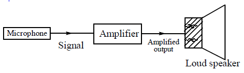
Amplifier has wide applications in industrial , T.V, radio and communication systems.
Amplifier :
The device which increases the weak input signal into strong output signal is called an amplifier.
Amplifiers are of two types
1) Power amplifiers
2) Voltage amplifiers
1) Power amplifier: Amplifier which is used to raise the power level is known as “Power amplifier.”
2) Voltage amplifier: The amplifier which is used to raise voltage level is known as voltage amplifier.
The most commonly used circuit for amplifier is common emitter circuit.
In this circuit, the battery VBB provides the biasing voltage VBE for the base emitter junction. A potential difference VCE is maintained between collector and emitter by the battery VCC. The emitter junction is forward biased and the collector junction is reverse biased. Most of the electrons from emitter cross the base region and move into the collector.
As shown in figure the input signal to be amplified is connected in series with the biasing battery (VBB). A load resistance (RL) is connected in the collector circuit. As the potential difference (VBE) changes with time due to input signal, base current (IB) changes. Due to this there will be large change in collector current IC and output voltage (VCE).
i) Voltage gain: It is defined as the ratio of change in output voltage to the change in input voltage.
Negative sign indicates input and output voltages are in opposite phase.
ii) Power gain: It is defined as the ratio of output power to the input power.
Power gain = AP = current gain ⨯ voltage gain
Note: In common base amplifier, the phase difference between the input and output signals is zero. In common emitter amplifier, the phase difference between the input and output signals is π.
33. BOOLEAN ALGEBRA
An English mathematician George Boole developed an ‘Algebra of Logic’, which is called ‘Boolean Algebra’ in his honour. It is based on human reasoning and is ideal for the design and analysis of logic circuts used in computers.
The main feature of this algebra is that it permits only two values or states for its variables. These two states may be ‘TRUE’ or “FALSE’ in logic, ‘ON’ or ‘OFF’ in electronic circuits but in mathematical way these are ‘1’ and ‘0’. Thus each Boolean variable can assume only one of the values 0 or 1.
Boolean algebra differs from both ordinary algebra (in decimal arithmetic system) and binary algebra (in binary arithmetic system).
e.g., we consider equation A + B = Y.
If A = 1 and B = 1, then
In Boolean algebra, 1+ 1=1, i.e., Y = 1
In binary algebra, 1+ 1 = 10, i.e., Y = 10
(read as one zero, not as ten.)
In ordinary algebra, 1+ 1=2, i.e., Y = 2
However, Boolean algebra uses two numbers, 0 and 1, appearing as mathematical symbols, but actually it is an algebra of words or ideas, not of numbers.
34 FUNDAMENTAL OPERATIONS OF BOOLEAN ALGEBRA
Boolean algebra uses only three basic operations on its variables:
(i) OR (ii) AND (iii) NOT
OR Operation : It is represented by the symbol ‘+’. In Boolean algebra, ‘+’ does not denote addition as in ordinary algebra. Here in symbolic logic it denotes the OR operation. In logic algebra A + B = Y means that when A is true OR B is true OR both are true, then Y will be true. The laws of OR operation may be expressed as
0 + 0 = 0, 0 + 1 = 1, 1 + 0 = 1, 1 + 1 = 1
AND Operation : It is a represented by the symbol ‘X’ or by ‘‘
In Boolean algebra ‘‘ does not denote multiplication as in ordinary algebra. Here in symbolic logic it denotes the AND operation. In logic algebra A. B = Y means that output C is true only when both A AND B are true. The laws of AND operation may be expressed as
0 . 0 = 0, 0 . 1 = 0, 1 . 0 = 0, 1 . 1 = 1
NOT Operation : It is a complementary operation and its symbol is an over bar.
In logic algebra Y = means if A is true then Y is not true. The laws of NOT operation may be expressed as
35. POSTULATES AND THEOREMS OF BOOLEAN ALGEBRA
OR laws
(1) A + 0 = A, (2) A + 1 = 1
(3) A + A = A, (4)
AND laws
(5) A . 0 = 0, (6) A . 1 = A
(7) A . A = A, (8) = 0
Complementation laws
(9) = 1, (10) , (11)
Commutative laws
(12) A + B = B + A, (13) A.B = B.A
Associative laws
(14) A + (B + C) = (A + B) + C
(15) A . (B . C) = (A. B).C
(16) A. (B + C) = AB + AC
(17) A + (B. C) = (A + B).(A +C)
Absorptive laws
(18) A + A.B = A, (19) A ( A + B) = A
(20) A + (.B) = A + B
(21) A.( +B) = A. B
De-morgan’s theorems :
(22)
(23)
(24)
(25)
36. BOOLEAN FUNCTIONS
OR Function : Y = A OR B i.e.
Y = A + B
Here, Y is a function of two Boolean variables A and B and is called as OR function of two variables A and B.
AND Function : Y = A AND B i.e.
Y = A . B
Here, Y is called as AND function of two variables.
NOT Function : Y =
Here, Y is called as NOT function of a single variable A.
NOR Function : Y = NOT (A OR B)
Here, Y is called as NOR function of two variables A and B. This also may be written as
.
NAND Function : Y = NOT (A AND B) is called as NAND function of two variables. This also may be written as
Identity Function : Y = NOT (NOT A) (i.e., ) is called Identity Function.
37. LOGIC GATES
A logic gate is an electronic circuit which evaluates a particular logical funcion. The circuit has one or more input terminals and an output terminal. A potential of zero (equal to the earth’s potential in general) denotes the logical value 0 and a fixed positive potential V (say, +5V) denotes the logical value 1. Each input terminal
denotes an independent variable. If zero potential is applied to an input terminal, the corresponding independent variable takes the value 0. If the positive potential V is applied to the terminal, the corresponding variable takes the value 1. The potential appearing at the output terminal denotes the value of the function. If the potential is zero, the value of the function is 0. If it is V, the value of the function is 1.
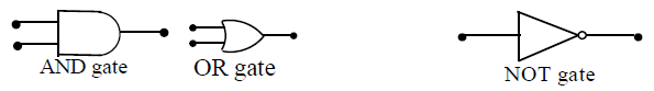
Figure shows the symbols for the logic gates to evaluate the functions AND, OR and NOT. They are known as AND gate, OR gate and NOT gate respectively. The terminals shown on the left are the input terminals and terminal on the right is the output terminal in each case.
Realisation of AND and OR gates with diodes
38. OR Gate
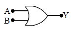
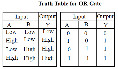
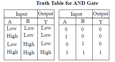
The OR gate has two or more inputs and one output. The two inputs have been marked as A and B and the output as Y. These variable A, B and Y have only one of the two values. i.e., either 0 or 1.
The OR Gate has an output 1 when either A or B or both A and B are 1. Obviously the output would be 0 if both inputs are 0. The OR Gate in terms of Boolean expression is A + B = Y The meaning of this equation is that Y is true when either A is true or B is true or both are true.
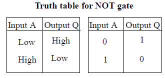
Truth Table
“A table which gives the output states for all possible inputs.”
Truth Table for OR Gate
We may interpret this with the help of equivalent circuits. Suppose ‘0’. shows that switch is open and ‘1’ shows that switch is closed. Also ‘0’ shows lamp is OFF and ‘1’ shows lamp is ON.
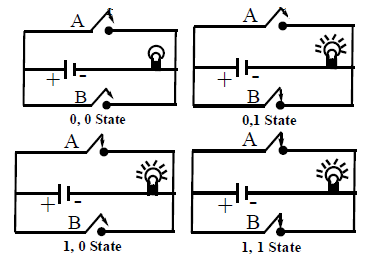
(i) When both inputs A and B are 0, both switches A and B are open. This implies circuit is incomplete and lamp is OFF, i.e., Y = 0.
(ii) When switch A is open and switch B is closed (A = 0 and B = 1), upper part of circuit is incomplete but lower part has complete circuit and as a result the lamp is ON (i.e.,Y = 1).
(iii) When switch A is closed and switch B is open (A = 1 and B = 0), Y = 1.
(iv) When A and B are closed. Both upper and lower circuits are complete, hence lamp is ON (A is 1 and B is 1, then Y is also 1).
Construction of OR gate by using diodes
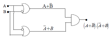
An OR gate may be constructed with two p-n junction diodes. The below figure shows the construction for an OR gate. The circuit evaluates the function Y = A OR B, i.e.,
∴ Y = A+B.
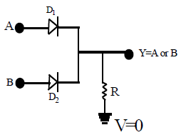
1. When A is at + 5 V, D1 is forward biased and hence conducts. The circuit current flows through R dropping + 5V across it; in this way Y achives potential +5 V. ( so output = 1)
2. When + 5V is applied to B, D2 conducts causing point Y to go to + 5V. (so output = 1)
3. When both A and B are +5 V, the potential drop across R is +5V because voltages A and B are in parallel. Again point Y is driven to + 5V. (so output is 1)
4. Obviously, when there are no voltages on either A or B, output remains 0.
39. AND Gate
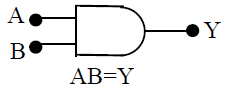
The AND circuit has two or more inputs and one output. Here also the two inputs have been marked as A and B while output as Y. A, B and Y are Boolean variables, i.e., having only two values, i.e., either 0 or 1. The AND Gate has an output 1 when its both A and B are 1.
The AND Gate in terms of Boolean expression is
A.B = Y
The logical meaning of this equation is that Y is true when both A and B are true.
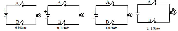
It is clear from equivalent circuits if both switches are closed (A =1, B=1), the lamp would be ON (Y=1). Even when one switch is open or both are open , circuit will not be complete , hence the lamp would be OFF ( i.e., Y= 0 in all other cases ).
Construction of an AND gate by using diodes
An AND gate may be constructed with two p-n junction diodes. The below figure shows the construction for an AND gate. The circuit evaluates the function Y = A AND B, i.e.,
∴ Y = A.B
1. When A is at 0 V and B is at + 5V, D1 is forward biased and hence conducts. The supply voltage +5 V drops across R. Consequently point P and Y is driven to zero potential. (so output = 0)
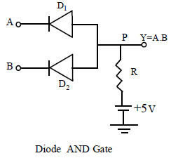
2. Similarly, when B is at 0 V and A is at +5V , D2 conducts and hence Y is driven to zero potential again. (So output = 0)
3. Obviously, when there is no voltage at either A or B, i.e ., both are at 0 V, both diodes conduct and again the output remains 0.
4. There is no supply of current and hence no drop across R only when both A and B are at +5V. Only in that case the output Y goes to supply a voltage of +5V. (So output = 1)
40. NOT Gate
The NOT circuit has one input and one output. It is called NOT Gate because output is not the same as its input.
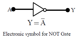
It inverts the polarity of the pulse applied to it. Thus NOT circuit negates the input function. When A is 0, Y is 1 and when A is 1, Y is 0 . In terms of Boolean Algebra Y= , where bar over A represents NOT A.
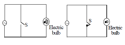
Let S be a switch connected in parallel with an electric bulb and a power source as shown in figure. When the switch is open the bulb glows. When the switch closed all the current flows through the switch and there is no current through the electric bulb. The bulb does not glow. Here, switch open represents zero (0) and closed represents 1. Bulb glows represents 1 and does not glow represents zero (0). The output is same as
that of a NOT gate.
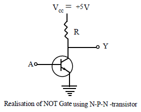
Realisation of NOT Gate with a transistor
A NOT gate cannot be constructed with diodes. The below figure shows a circuit using an n-p-n transistor to evaluate the NOT function.
When +5 V is applied to A, the transistor will be fully ON, drawing maximum collector current . Hence, whole of VCC = +5 V will drop across R, and potential at Y will be 0 V. If 0 V is applied at A, the transistor will be cut off and the output Y, therefore will be equal to VCC, i.e., +5V. Obviously in each case output is opposite of input.
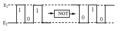
The NOT circuit inverts the waveform as shown below, but keeps the variable operation between the same two limits E1 and E2.
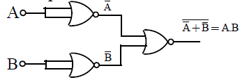
41. NOR Gate
If we put a NOT Gate at the output of OR Gate, we observe the results given in the following Truth Table.
Thus we obtain a very useful combination called as NOR Gate.
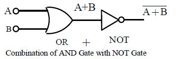
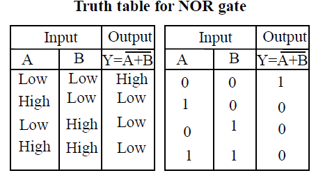
The Boolean equation for NOR Gate is
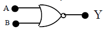
Electronic symbol for two input NOR Gate
This gate is very useful because we may obtain all the possible gates by using this NOR Gate as basic building block. This is why NOR Gate is called as a universal gate.
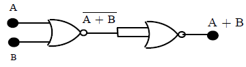
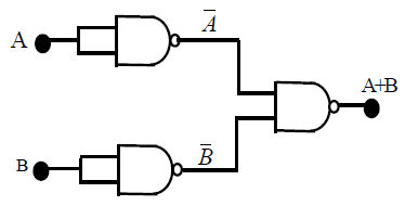
42. CONSTRUCTION OF NOT GATE BY USING NOR GATE.
A NOR Gate has two inputs and one output. If we combine both the inputs we get one input and one output device . Let us consider the truth tables of this combination.
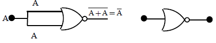
|
Input A |
Output Q |
|
0 1 |
1 0 |
We observe that outputs obtained are just inversions of inputs. In terms of Boolean expression we get.
Which is Boolean expression for NOT Gate.
43. CONSTRUCTION OF OR GATE BY USING NOR GATES
If we consider another combination, in which we put a NOT Gate (obtained from NOR Gate as above ) at the output of NOR Gate, we get two input and one output device. Let us consider the truth table of this combination.
Also in terms of Boolean algerbra.
which is Boolean equation of OR Gate.
Note: An OR gate can be constructed by using two NOR gates.
44 CONSTRUCTION OF AND GATE BY USING NOR GATES
If we consider another combination , in which we put NOT Gates (obtained from NOR Gate as above ) in both the inputs, we get two input and one output device . Let us consider the truth table of this combination.
Also in terms of Boolean algebra,
(using De Morgan’s theorem) which is Boolean expression for AND Gate.
Note: An AND gate can be constructed by using three NOR gates.
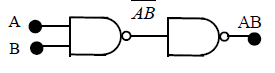
45. NAND Gate
Put a NOT Gate in the output of an AND Gate and analyse the results of the following truth table:
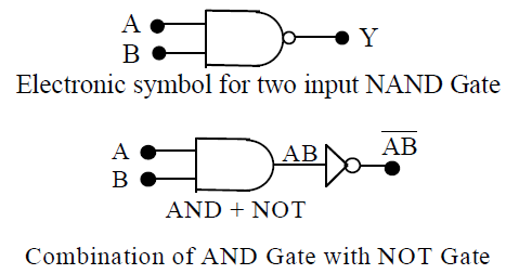
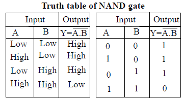
Thus we get further a very useful combination called as NAND Gate. Boolean equation for NAND Gate is
NAND Gate is called as universal gate. NAND Gate may also be used to realise the basic logic functions; OR, AND and NOT.
46. CONSTRUCTION OF NOT GATE USING NAND GATES
If both the inputs of a NAND Gate are combined, we get single output device resulting in NOT Gate.
Consider the truth table:

In terms of Boolean algebra,
which is Boolean expression for NOT Gate.
47. CONSTRUCTION OF OR GATE USING NAND GATES
we put NOT Gates (obtained from NAND Gate as above ) in both the input of NAND Gate. We get two input and one output device resulting an OR gate
In terms of Boolen equation
Note: An OR gate is constructed by using three NAND gates.
48. CONSTRUCTION OF AND GATE USING NAND GATES
If a NOT Gate (obtained from NAND Gate as above ) is put at the output of NAND Gate, we get two input and one output device resulting an AND gate
In terms of Boolen equation
Note: AND gate can be constructed by using two NAND gates.
49. ELECTRICAL REISSTIVITY OF SEMICONDUCTORS
Consider a block of semiconductor of length l, area of cross-section A and having number density of electrons and holes as ne and nh respectively. Suppose that on applying a potential difference, say V, a current I flows through it as shown in figure. The electron current (Ie) and the hole current (Ih) constitute the total current I flowing through the semiconductor i.e., …………(1)
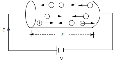
If ne is the density of conduction band electrons in the semiconductor and ve is the drift velocity of electrons, then electron current is given by ……(2)
Also, the hole current, ……….. (3)
Using the equation (2) and (3), the equation (1) becomes
or ………..(4)
If is the resitivity of the material of the semiconductor, then the resistance offered by the semiconductor to the flow of current is given by
… (5)
Since V = RI, from the equations (4) and (5), we have
or ……… (6)
If E is the electric field set up across the semiconductor, then ……. (7)
From the equations (6) and (7), we have
or …………. (8)
On applying electric field, the drift velocity acquired by the electrons (or holes) per unit strength of electric field is called mobility of electrons (or holes).
Therefore, the equation (8) becomes
………… (9)
Also, is called the conductivity of the material of semiconductor.
……………… (10)
It may be pointed out that electron mobility is higher than hole mobility. The mobility of electrons and holes depend weakly on temperature and is independent of their density. The change in conductivity of a semiconductor is mainly due to changes in carrier concentration.
50. INTRINSIC CONCENTRATION
The density of a hole electron pair increases with increase in temperature (T). As a result conductivity increase. The intrinsic concentration ni varies with T as
Where Eg is the forbidden energy gap at 0 K in electron – volt, k is Boltzmann’s constant in eV/K and A0 is a constant.
With a rise in temperature there are increased thermal lattice vibrations due to which resistance increases. But in case of semiconductors the number of charge carriers increases very rapidly with rise in temperature. The overall effect is increase in conductivity of semiconductor.
51. THE ENERGY GAP
Experimentally it has been found that the forbidden energy region Eg depends on temperature.
For silicon, Eg (T) = 1.21 – 3.60 x 10⁻⁴ T
For germanium, Eg (T) = 0.785 – 2.23 x 10⁻⁴ T
At room temperature (300 K),
For silicon, Eg=1.1 eV
For germanium, Eg = 0.72 eV
Adding equal concentrations of donor and acceptor atoms to P-type and N- type semiconductor respectively results in an intrinsic semiconductor.
When concentration of donor atoms exceeds the acceptor concentration in a P-type semiconductor, it is changed from a P-type to an N-type semiconductor.
52. GENERAL THEORY OF FEEDBACK
The general theory of feed back can be understood with the help of block diagram shown in the figure. The feedback amplifier has two parts, i.e., amplifier and feed back circuit. The feedback circuit usually consists of resistors. This returns a fraction (say β ) of the output voltage back to the input. Let A be the gain of the amplifier, i.e., the ratio of output voltage V0 to the input voltage Vi. This is the gain of the amplifier without feedback. The feedback network extracts a voltage Vf = βV0 from the output V0 of the amplifier. This voltage is added (positive feedback) or subtracted (negative feedback) from the signal voltage VS. Now
(Positive feedback)
(Negative feedback)
The quantity is called as feedback ratio or feed back fraction. Let be the overall gain(gain with feedback) of the amplifier. This is defined as the ratio of output voltage V0 to the applied signal voltage VS
Thus, gain without feedback
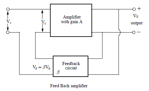
or ………. (1)
Further ………… (2)
From eqs. (1) and (2), we get
or
……. (3)
But the resultant gain of the amplifier with feed back
……… (4)
From eqs (3) and (4)
positive feedback ……….. (5)
negative feedback
Now we consider the following three cases:
i) When , feedback is negative.
ii) When , feed back is positive.
iii) Considering the case of positive feedback, if . This is possible only when input is zero.
Thus, the amplifier is then capable of producing output even when input is zero. Under this situation, amplifier works as an oscillator.
The condition Aβ = 1 is called as Berkhausen condition for oscillations.
53. OSCILLATORS :
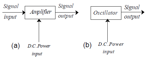
An oscillator is an electronic circuit associated with a transistor that provides an alternating output while deriving its input from a direct current source. Thus it converts d.c. into a.c. and, therefore, also called an inverter.
An oscillator generates alternating voltages or currents over a wide frequency range, from a few cycle per hour to millions of cycles per second. The oscillator is an essential part of the radio communication system and finds its use in radio and T.V. transmitters and receivers. The function of an oscillator is similar to that of an amplifier. However, there is a basic difference between an amplifier and an oscillator. An amplifier produces an output signal whose waveform is similar to the input signal but whose power level is generally high. This additional power is supplied by the external d.c. source. Thus in an amplifier, the frequency, waveform and magnitude of the a.c power generated is controlled by an a.c. input signal. If there is no input signal, there is no output signal and hence there is no energy conversion. On the other hand, in an oscillator, the frequency, waveform and magnitude of the a.c. power generated is controlled by the circuit itself and it does not require an external signal either to start or maintain energy conversion process. Thus an oscillator is an amplifier which provides its own input signal. It keeps producing an output signal so long as the d.c. power source is connected, as shown in figure 16.34(b).
54. ESSENTIALS OF TRANSISTOR OSCILLATOR
Figure shows the essential components of the oscillator which are
(i) Tank Circuit : A simple circuit consisting of an inductance L and a capacitor C in parallel constitutes a tank circuit. In which magnetic energy oscillates with finite frequency. The oscillatory process goes on repeating itself and an oscillatory current is produced in the L-C circuit.
The values of L and C components determine the frequency of oscillation of the circuit. The frequency of oscillation
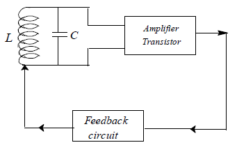
(ii) Transistor Amplifier : It changes the d.c. power received from the capacitor into a.c. power and supplies output as well as to the tank circuit to meet the losses.
(iii) Feedback circuit : It provides a positive feedback i.e., it supplies a part of collector energy to the tank circuit in correct phase to maintain the oscillations there.
(i) Transistor as a switch :
When the transistor is used in the cutoff or saturation state it acts as a switch. On the other hand for using the transistor as an amplifier, it has to operate in the active region.
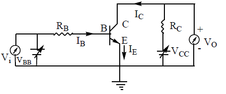
Let us try to understand the operation of the transistor as a switch by analysing the behaviour of the base-biased transistor in CE configuration as shown in figure.
Applying Kirchoff’s voltage rule to the input and output sides of this circuit, we get
We shall treat VBB as the dc input voltage Vi and VCE as the dc output voltage V0. So we have
Let us see how V0 changes as Vi increases from zero onwards. In the case of Si transistor, as long as input Vi is less than 0.6V, the transistor will be in cut off state and current IC will be zero.
Hence V0 = VCC
Let us see now how the transistor is operated as a switch. As long as Vi is low and unable to forward-bias the transistor, V0 is high (at VCC). If Vi is high enough to drive the transistor into saturation, then V0 is low, very near to zero. When the transistor is not conducting it is said to be switched off and when it is driven into saturation it is said to be switched on. This shows that if we define low and high states as below and above certain voltage levels corresponding to cutoff and saturation of the transistor, then we can say that a low input switches the transistor off and a high input switches it on. Alternatively, we can say that a low input to the transistor gives a high output and a high input gives a low output. The switching circuits are designed in such a way that the transistor does not remain in active state.
55. PHOTO DIODE
A photo diode is essentially a reverse biased P-N junction diode which is designed to respond to light absorbed.
(a) Principle : A reverse biased P-N junction diode has a reverse saturation current which is mainly due to the flow of the minority carriers. If light is allowed to fall on such a reverse biased P-N junction diode, additional electronhole pairs are generated in both P and N regions. It produces a very large change in minority carrier concentration and hence increases the reverse current through the diode. It is found that the current through the diode varies almost linearly with the light flux. Hence light can be detected using a reverse biased P-N junction diode known as photo diode
(b) Construction :
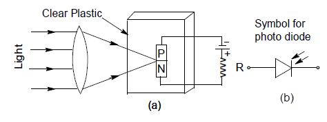
A photo diode consists of a P-N junction embedded in a clear plastic capsule as shown in fig. Radiation is allowed to fall upon one surface across the junction. Sometimes, a lens is placed on the junction side of the photo diode to focus the incident light on the surface for maximum activity. All the sides of the plastic capsule, except the illuminated one, are either painted black or enclosed in a metallic case. The semiconductor photo diode is extremely small and has dimensions of the order of a few mm. Figure shows the schematic symbol for a photodiode. The inward arrows represent the incoming light.
(c) Working and characteristics : When photo diode is kept under dark condition and a sufficient reverse voltage is applied, then an almost constant current, independent of magnitude of reverse bias, is obtained. This current corresponds to the reverse saturation current due to thermally generated minority carriers and is called dark current because it flows when no light is incident. It is proportional to the concentrations of minority carriers (holes in N and electrons in P-region) and is denoted by Id. Majority charge carriers are not allowed to cross the junction barrier
under this reverse bias condition.
When light is allowed to be incident on the diode surface, additional electron hole pairs are formed. But since the concentration of majority carriers is much greater as compared to that of minority carriers, the percentage increase of majority carriers is much smaller than the percentage increase of minority carriers. Hence, we can neglect the increase in majority density and can consider the radiation entirely as minority carrier injector. These injected minority carriers diffuse to the junction, cross and contribute to the additional current. Thus under large reverse bias conditions, the total reverse current is given by I = Is + Id where Is is the short circuit current and is proportional to light intensity.
Figure 16.37 represents the volt-ampere characteristic curve for three different values of illumination (intensity) for photo diode.
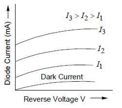
Only the curve representing the dark current passes through the origin. It may be seen that the current increases with increase in the level of illumination for given reverse voltage. Thus, the reverse current can be changed by changing the level of illumination. The reverse resistances of the diode can be changed likewise.
(d) Uses of Photo diode :
1. A photo diode can turn its current ON and OFF in nanoseconds, hence it is used where light is required to be switched OFF and ON at a very fast rate.
2. A photo diode is used in light detection, in light operated switches, reading of computer punched cards and tapes etc.
3. Photo diodes find tremendous application in optical communication system.
4. They find many uses in instrumentation, control, automatic and communication.
56. LIGHT-EMITTING DIODES (LED)
A light emitting diode (LED) is a specially made forward biased P-N junction diode which emits visible light when energised.
a) Theory : When a P-N junction diode is forward biased, the potential barrier is lowered and the majority charge carriers start crossing the junction. As soon as conduction band electrons from N-region cross the barrier and enter the P-region, they recombine with holes. Similarly, some holes from P-region, may try to cross the junction but a conduction band electron may fall into hole before the hole crosses the junction. In either case recombination of electrons and holes take place. Now since a definite amount of energy is required to generate an electron-hole pair, the same energy is released when an electron recombines with hole. If Eg is the of radiation, the corresponding emission wavelength is given
by
In case of Ge and Si the liberated energy goes into heating of the crystal and the amount of emitted light is insignificant.
In case of GaAs,
band gap and we get
which lies in the infrared region. The band gap of Gallium Arsenide Phosphide (Ga As P) is about 1.9 eV and the radiation is of 6500 Å which is visible (red or yellow amber). Thus by a proper choice of band -gap and the material, radiation of desired wavelength may be obtained. It is possible to obtain orange, yellow and green emissions.
Gallium phosphide (GaP) gives red or green light.
(b) Construction and Working
At first an N-type layer is grown on a substrate and then a P-type layer is deposited on it by the process of diffusion.
Metal contacts (Anode) are made at the outer edge of the P-layer so that more upper surface is left free for light to escape.
For making cathode connection, metal film (preferably gold) is coated at the bottom of the substrate. This film also reflects as much light as possible to the surface of the device.
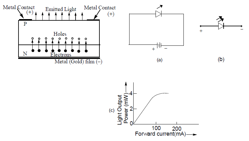
Such a specially made P-N diode (LED), gives emission in the visible region when forward biased. Figure16.39(b) shows the schematic symbol of LED and an important characteristics of LED. LED emits light when a sufficient forward current is applied. Figure 16.39(c) shows that greater the forward current, greater is the light output of the LED. Thus amount of power output converted into light is directly proportional to forward current. LEDs emit no light when reverse biased.
c) Uses of LEDS : Following are the important applications of LED :
1. The infrared LED finds applications in burglar alarm systems and other areas requiring invisible radiation.
2. LED that produce visible radiation find applications in numerical displays like watches, calculators, instrument panels, telephone switch boards etc. A seven segment display unit is made by using a number of LEDs.
3. The infrared LED is a potential source for optical fibre communication.
4. They are rapidly replacing cathode ray tubes in solid state video displays.
5.7 THE SOLAR CELLS :
A solar cell or solar battery is basically a P-N junction diode which converts solar energy into electrical energy. It is also called a solar energy converter and is simply a photo diode operated at zero bias voltage.
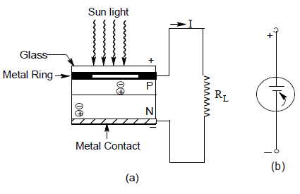
A solar cell consists of a P-N junction diode generally made of Ge or Si It may also be constructed with many other semiconducting materials like gallium Arsenide (Ga As), indium Arsenide (InAs) and cadmium arsenide (CdAs).
The P-N diode so formed is packed in a can with glass window on top so that light may fall upon P and N type materials. The thickness of the P-region is kept very small so that electrons generated in this region can diffuse to the junction before recombination takes place. Thickness of N-region is also kept small to allow holes generated near the surface to diffuse to the junction before they recombine. A heavy doping of P and N regions is recommended to obtain a large photo voltage. A nickel plated ring is provided around the P-layer which acts as the positive output terminal. A metal contact at the bottom serves as the negative output terminal. Figure 16.40(b) gives the schematic symbol of a solar cell. The invert arrow indicates the incoming light.
Working : The working of solar cell may be understood with reference to fig16.40. When light is allowed to incident on a P-N junction diode, photons collide with valence electrons and impart them sufficient energy enabling them to leave their parent atoms. Thus electron- hole pairs are generated in both the P and the N-sides of the junction. These electrons and holes reach the deflection region W by diffusion and are then separated by the strong barrier field existing there. However, the minority carriers, electrons in the P-side slide down the barrier to reach the N-side and the holes in the N-side move to P-side. Their flow constitutes the minority current which is directly proportional to the illumination and also depends on the surface area being exposed to light. The accumulation of electrons and holes on the two sides of the junction gives rise to an open circuit voltage VOC which is a function of illumination. The opencircuit voltage produced for a silicon solar cell is typically 0.6 volt and the short circuit current is about 40 mA/cm2 in bright noon day sum light. Many such cells are interconnected to provide large quantities of electrical power. Solar panels providing 5 watt at 12 volt have been built to operate 24 hours a day by recharging the batteries during day light hours.
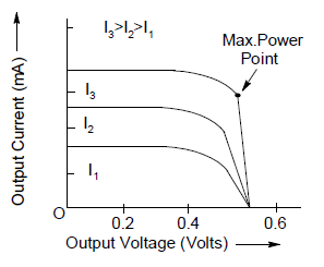
Typical V-I characteristics of a solar cell, corresponding to different levels of illumination are shown in fig16.41. It may be seen that for 100m W/cm2 illumination, the open circuit voltage is about 0.57 volt while the short circuit current is 50 mA. Maximum power output is, however obtained when the cell is operated at the knee of the curve.
Uses of solar cell : Solar cells are used extensively in satellites and space vehicles to supply power to electronic and other equipments or to charge storage batteries. They are receiving attention even for terrestrial electric power generation.
SOLVED EXAMPLES
1. The energy of a photon of sodium light (λ = 589nm) equal to the band gap of a semiconducting material. (a) Find the minimum energy E required to create a hole-electron pair. (b) Find the value of E/kT at a temperature of 300 K.
Sol. (a) The energy of the photon in eV =
Wavelength of photon = 589 nm = 5890Å
Thus the band gap is 2.1 eV. This is also the minimum energy E required to push an electron from the valence band into the conduction band. Hence, the minimum energy required to create a hole-electron pair is 2.1eV
(b) At T = 300K, kT =
=
Thus,
The available thermal energy is nearly 81times less than that of the required energy to create electron hole pair. So it is difficult for the thermal energy to create the hole-electron pair but a photon of light can do it easily.
2. Pure Si at 300 K has equal electron (ne) and hole (nh) concentration of . Doping by indium increases into . Calculate ne in the doped silicon.
Sol. Here
But
3. Find maximum voltage across AB in the circuit shown in Fig. Assume that diode is ideal.
Sol. As the diode is treated ideal, its forward resistance Rf = zero.
It acts as short circuit. So, 10 kΩ is in parallel with 15kΩ and the effective resistance across AB is
6kΩ is in series with 5kΩ
∴ total resistance =
V = 30V. Current drawn from the battery is
4. In the given circuit diagram.VB = 0.6 V
(a) Calculate the current i in the circuit.
(b) Find the current (I) if the diode is reversed.
Sol. (a)
(b) i = 0 since diode is reverse biased (open circuited).
5. In a p-n junction diode, the depletion region is 400nm wide and an electric field of V/m exists in it. The minimum kinetic energy of a conduction electron which can diffuse from n side to p side is
Sol. The p.d across the junction V=Ed
But change in K.E. = work done
∴ the K.E required to conduct electron from n side to p side= V electron volts
6. Two junction diodes, one of germanium (Ge) and other of silicon(Si) are connected as shown in fig to a battery of 12V and a load resistance 10kΩ . The germanium diode conducts at 0.3V and silicon diode at 0.7V. When current flows in the circuit, the potential of terminal Y will be
Sol. The Ge diode conducts for a p.d of 0.3V, therefore the current passes through it and the Si diode do not conduct.
Hence the potential of terminal Y = 12-0.3 = 11.7V
7. In the circuit shown, the potential drop across each capacitor is (assuming the two diodes are ideal)
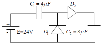
Sol. The diode D1 is reverse biased(open circuit), but the diode D2 is forward biased(short circuit).
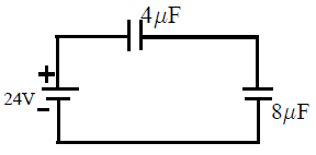
∴ the potential of the battery divides across the two capacitors in the inverse ratio of their capacities. i.e.
8. A potential barrier of 0.50 V exists across a p-n junction. (a) If the depletion region is m wide, what is the intensity of the electric field in this region ? (b) An electron with a speed of m/s approaches the p-n junction from the n-side. With what speed will it enter the p-side ?
Sol (a) The electric field is E = V/d
(b)
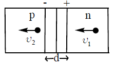
Suppose the electron has a speed v1 when it enters the depletion layer and v2 when it comes out of it. As the potential energy increases by e⨯0.50 V, from the principle of conservation of energy.
Solving this, .
9. The circuit shown in Fig. contains two diodes each with a forward resistance of 50 ohm and with infinite reverse resistance. If the battery voltage is 6 V, find the current through the 100 ohm resistance.
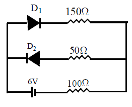
Sol. As per given circuit, diode D1 is forward biased and offers a resistance of 50 ohm. Diode D2 is reverse biased and as its corresponding resistance circuit is as shown in Fig.As all the three resistances are in series, the current through them is
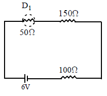
10. The applied input ac power to a half wave rectifier is 100 W. The dc output power obtained is 40W. Find the rectifier efficiency.
Sol. ac input power = 100 W; dc output power = 40 W.
= 0.4
∴ Percentage efficiency of the half wave rectifier = 40%
11. A p-n diode is used in a half wave rectifier with a load resistance of 1000Ω. If the forward resistance (rf) of diode is 10Ω, calculate the efficiency of this half wave rectifier.
Sol. Load resistance RL = 1000Ω ; Forward resistance of the diode = rf = 10Ω.
Efficiency of half wave rectifier
The percentage efficiency of the half wave rectifier = 40.19%
12. A full wave rectifier uses two diodes with a load resistance of 100Ω. Each diode is having negligible forward resistance. Find the efficiency of this full wave rectifier.
Sol. Forward resistance of the diode, rf = 0Ω ; Load resistance, RL = 100Ω;
Efficiency of full wave rectifier
The percentage efficiency of the full wave rectifier = 81.2%
13. The current through a P-N junction diode is 55mA at a forward bias voltage of 3.0 V. If the temperature is 27°C, find the static resistance of the diode.
Sol. The static resistance
14. Considering the circuit and data given in the diagram, calculate the currents flowing in the diodes D1 and D2.
Forward resistance of D1 and D2 is 20Ω.
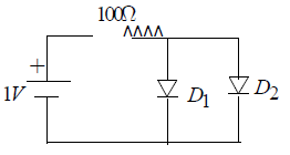
Sol. Since the positive terminal of battery is connected to P-type of both diodes D1 and D2, they are forward biased. These diodes are replaced by with their forward resistances as shown in Fig.
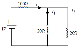
The resistance of 20Ω and 20Ω in parallel
Therefore, total current I in the circuit
and
15. If a p-n junction diode, a square input signal of 10V is applied as shown,

then the output signal across RL will be
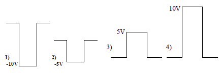
Sol. The junction diode will conduct when it is forward biased. Therefore, the output voltage will be obtained during positive half cycle only. So correct option is (3).
16. For the circuit shown in Fig. find
1) the output voltage;
2) the voltage drop across series resistance;
3) the current through Zener diode.
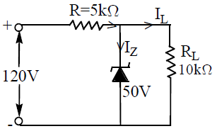
Sol. From the figure
Input voltage
zener voltage,
1) Output voltage,
2) Voltage drop across series resistance
3) Load current
Current through
According to the Kirchhoff’s first law I = IL + IZ
∴ Zener current,
17. A zener diode has a breakdown voltage of 9.1 volts with a maximum power dissipation of 364 milliwatts. What is the maximum current the diode can handle?
Sol.
18. In a single state transistor amplifier, when the signal changes by 0.02 V, the base current change by 10μA and collector current by 1mA. If collector load RC = 2kΩ and RL = 10kΩ, Calculate : (i) Current Gain (ii) Input impedance, (iii)Effectivea.c.load, (iv) Voltage gain and (v) Power gain.
Sol. (i) Current Gain
(ii) Input impedance
(iii) Effective (a.c) load
(iv) Voltage gain
(v) Power gain, AP = Current gain × Voltage gain
= 100 × 83 = 8300
19. A p-n-p transistor is used in common-emitter mode in an amplifier circuit. A change of 40μA in the base current brings a change of 2 mA in collector current and 0.04 V in base-emitter voltage. Find the : (i) input resistance (Rin) and (ii) the base current amplification factor (β).
If a load of 6kΩ is used, then also find the voltage gain of the amplifier.
Sol. Given
(i) Input Resistance,
(ii) Current amplification factor,
(iii) Voltage gain in common-emitter configuration.
20. For a transistor β = 40 and IB = 25μA . Find the value of IE .
Sol. (If only d.c. values are considered)
21. In a transistor β = 45 , the change in the voltage across 5 kΩ resistor which is connected in collector circuit is 5V. Find the change in base current.
Sol. Change in the collector current
But
Change in base current
22. Current amplification factor of a common base configuration is 0.88. Find the value of base current when the emitter current is 1 mA.
Sol. In a common-base arrangement, the current amplification factor.
Given
∴ Collector current
Now since
∴ Base current
23. In a transistor, the emitter circuit resistance is 100Ω and the collector resistance is 100kΩ . The power gain, if the emitter and collector currents are assumed to be equal, will be
Sol. If
24. In the following common-emitter configuration an n-p-n transistor with β = 100 is used. The output voltage of the amplifier will be

Hint :
25. An n-p-n transistor in a common emitter mode is used as a simple voltage amplifier with a collector current of 4mA. The terminal of a 8 V battery is connected to the collector through a load resistance RL and to the base through a resistance RB. The collector-emitter voltage VCE = 4 V, base-emitter voltage VBE = 0.6 V and base
current amplification factor βd.c = 100 . Calculate the values of RL and RB
Sol. Potential difference across RL
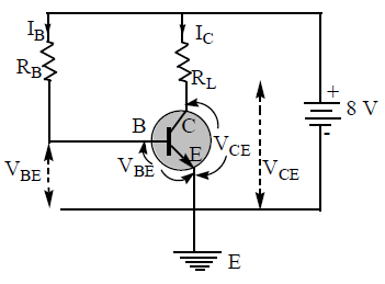
= 8V – VCE
= 8V – 4V
= 4V
Now ICRL= 4V
Further for base emitter equation,
or IBRB = Potential difference across RB
Again,
26. The Boolean expression of the output Y of the inputs A and B for the circuit shown in the fig
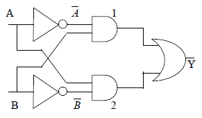
Sol. The output of AND gate 1 is
The output of AND gate 2 is
∴ the output of OR gate is,
27. The combination of NAND gates shown here under are equivalent to
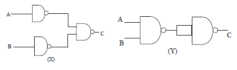
Sol. For the combination of gates in (X), the bollean expression is
For the combination of gates in (Y), the bollean expression is
28. The diagram of a logic circuit is given below. The output of the circuit is represented by
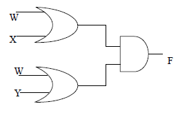
Sol. F = (W+X).(W+Y)
= W.W+W.Y+X.W+X.Y
= W+W.Y+X.W+X.Y
= W(1+Y)+XW+X.Y
= W+XW+X.Y
= W(1+X)+X.Y=W+X.Y
29. The logic circuit and its truth table are given, what is the gate X in the diagram
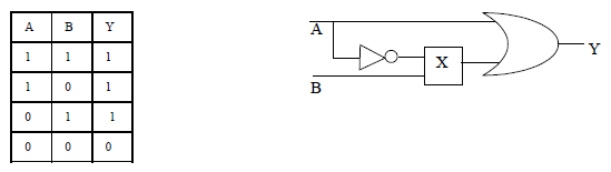
Sol. From the truth table we note that Y=A+B
i.e, it is for OR gate (or)
A + X = A + B = A + B.
then, A + X = A + B.A +
So X = .B , which is AND gate with inputs as and B.
30. Draw the logic circuit corresponding to the boolean expression.
Sol. It is an expression showing sum of two products. Thus we require two AND gates and an OR gate. To generate we also require a NOT gate. Their circuit can be drawn as follows.
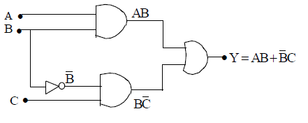
31. SimplifyY = AB + ABC + B + AC using Boolean Algebra. Draw the resultant simplified logic circuit.
Sol. Given
Logic Circuit is shown below.
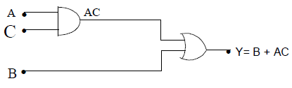
32. Write Boolean equation for the output of fig. and solve this equation for all possible input conditions.
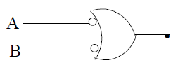
Sol. The Boolean equation for the output of fig.
(i) When A = 0 B = 0 then Y = + = 1 + 1 = 1
(ii) When A = 0, B = 1,
then, Y = = 1 + 0 = 1
(iii) When A = 1, B = 0,
then
(iv) When A = 1, B = 1,
then
Hence
Draw logic diagrams for the Boolean expressions given below.
(i) (ii)
Sol. (i) The required logic diagram for the given Boolean expression is given in figure. Here the input B before applying to first AND gate and input A before applying to second AND gate have been inverted. The output of these gates are, therefore, and respectively. These outputs are fed to OR gate which gives as
shown in figure.
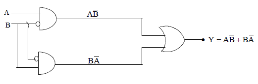
ii) The required logic diagram for the given Boolean expression is shown in figure. The input B to first OR gate and input A to second OR gate have been inverted. The output of these gates are, therefore, as shown. These inputs when applied to AND gate give the required output.